


Texas Instruments SN74LVC1G34/SN74LVC1G34-Q1 Single Buffer Gates
Texas Instruments SN74LVC1G34/SN74LVC1G34-Q1 Single Buffer Gates are designed for operation with a VCC range of 1.65V to 5.5V. It performs the Boolean function Y = A in positive logic. The CMOS device has high output drive while maintaining low static power dissipation over a broad VCC operating range. This device is fully specified for partial-power-down applications using Ioff. The Ioff circuitry disables the outputs, preventing damaging current backflow through the device when it is powered down. The SN74LVC1G34/SN74LVC1G34-Q1 is available in various packages, including the ultra-small DPW package with a body size of 0.8mm × 0.8mm. The Texas Instruments SN74LVC1G34-Q1 devices are AEC-Q100 qualified for automotive applications.
Features
- Available in the ultra-small 0.64mm2 package (DPW) with 0.5mm pitch
- Supports 5V VCC operation
- Inputs accept voltages to 5.5V
- Provides down translation to VCC
- Maximum tpd of 3.5ns at 3.3V
- Low power consumption, 1µA maximum ICC
- ±24mA output drive at 3.3V
- Ioff supports live insertion, partial power down mode, and back drive protection
- Latch-up performance exceeds 100mA per JESD 78, Class II
- ESD protection exceeds JESD 22
- 2000V human-body model (A114-A)
- 200V machine model (A115-A)
- 1000V charged-device model (C101)
Applications
- AV receiver
- Audio dock (portable)
- Blu-ray player and home theater
- DVD recorder and player
- Embedded PC
- MP3 player/recorder (portable audio)
- Personal Digital Assistant (PDA)
- Power in a telecom/server AC/DC supply (single controller (analog and digital)
- Solid State Drive (SSD) (client and enterprise)
- TV (LCD/digital and high-definition (HDTV))
- Tablet (enterprise)
- Video analytics (server)
- Wireless headset, keyboard, and mouse
Datasheets
Functional Block Diagram

Development Tool
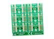
Texas Instruments 5-8-LOGIC-EVM Evaluation Module
Developed to support leaded Logic devices in the DBV, DCK, DCT, DCU, and DRL packages.
Publicerad: 2025-09-29
| Uppdaterad: 2025-10-06